Descriptive part
Atelier Interuniversitaire de Micro-nano Électronique (AIME)
AIME is a structure permanently accessible to academics and industrialists, equipped with computer-aided design (CAD) and heavy technological equipment in clean rooms necessary for the manufacture and testing of integrated devices and circuits on silicon.
The objective is to realize a gas sensor based on WO3 nanoparticles and then to evaluate it under controlled gas atmosphere to provide the datasheet. The process then breaks down into 4 major steps:
- Synthesis of WO3 nanoparticles
- Elaboration of the microelectronic chip
- Integration of the sensitive layer of nanoparticles on the chip
- Electrical characterization of the sensor under controlled atmosphere
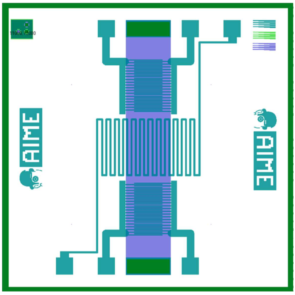
The chips produced consist of 4 components:
• A heating resistor embedded in n-doped poly-silicon
• An aluminum resistor for heating or measurement, located on the surface
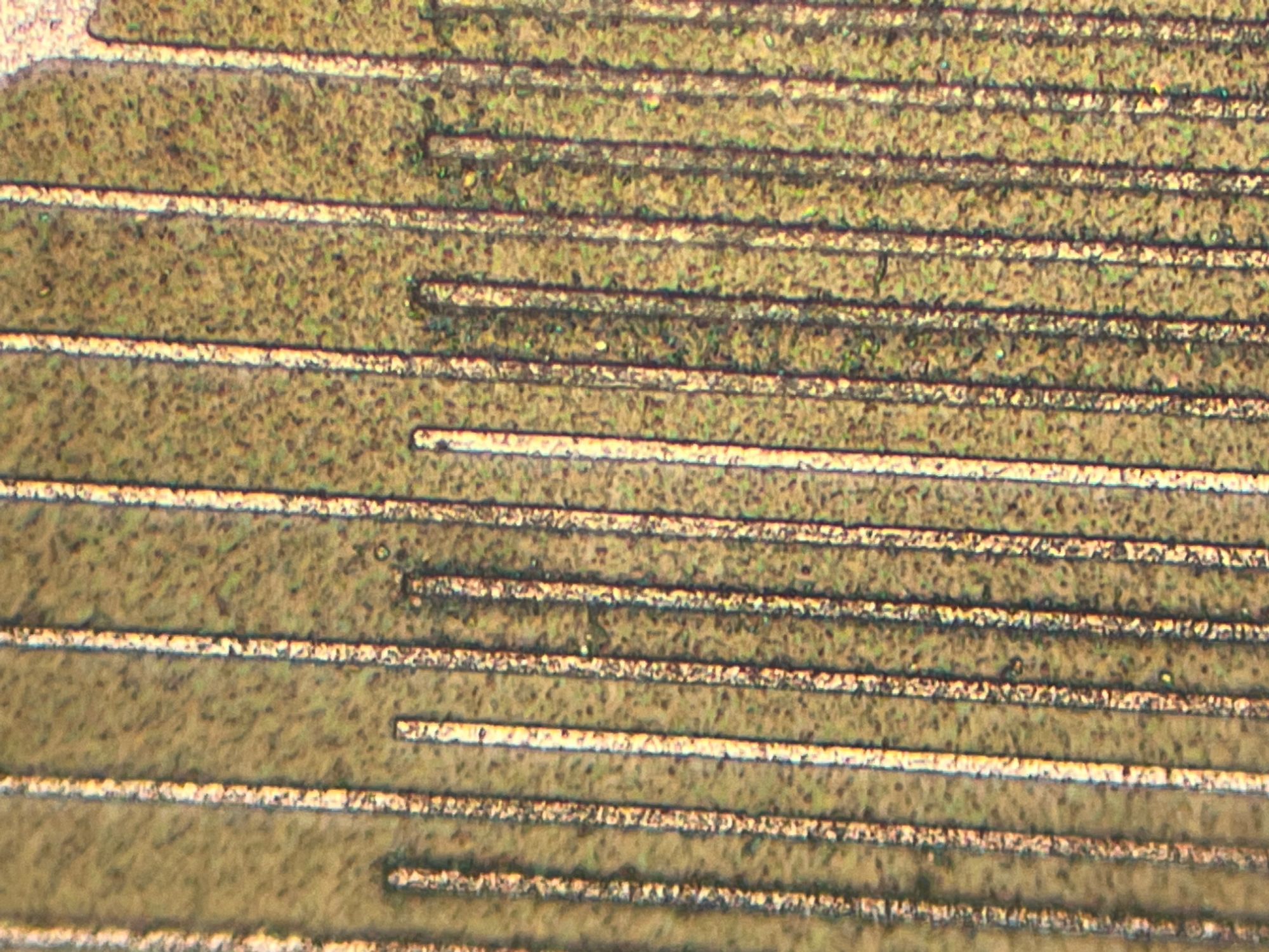
• Two interdigitated combs which will receive the layer of nanoparticles and which will become resistors sensitive to the gaseous environment.
The details of all the manufacturing steps are too long to appear here. I therefore refer you to the practical work booklet containing all the information. However, here are the main steps of the wafer manufacturing process:
- Masking oxidation
- Poly-Silicon deposit
- Poly-Silicon doping (N-type)
- Photoengraving N°1: Poly-Silicon engraving
- Deposition of a dry oxide layer
- Engraving N°2: Contact opening
- Metallisation
- PhotoEngraving N°3: Metal engraving
- Annealing metal
- Mounting
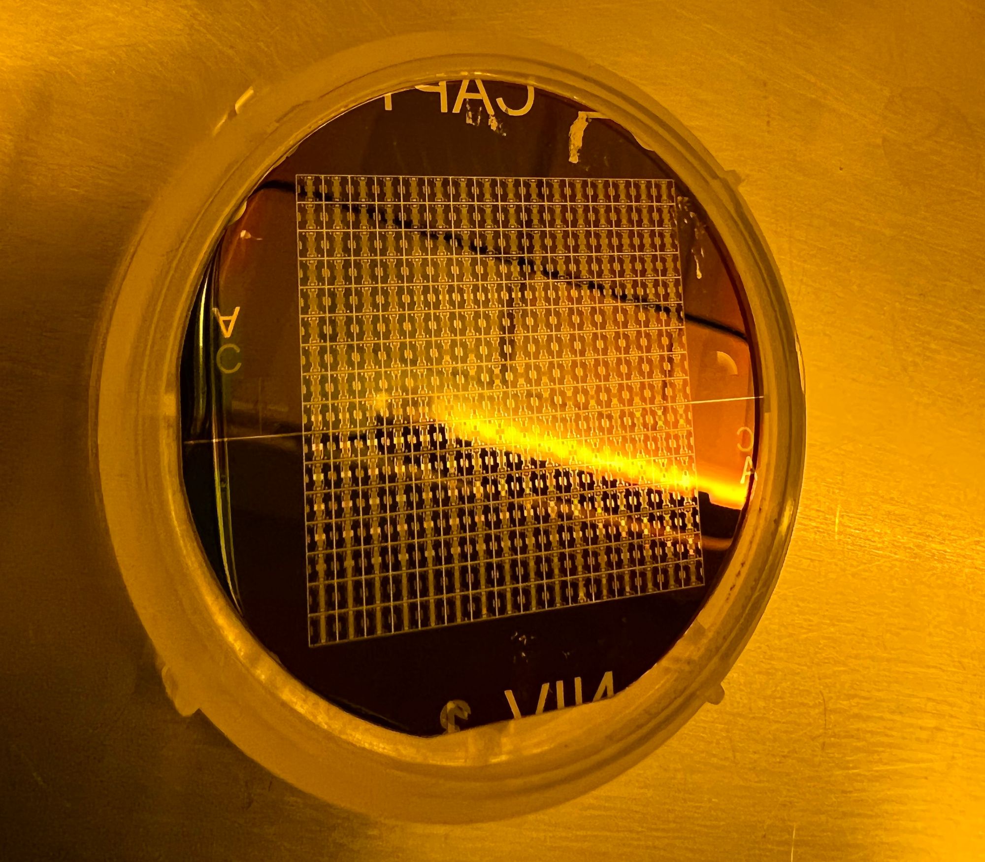
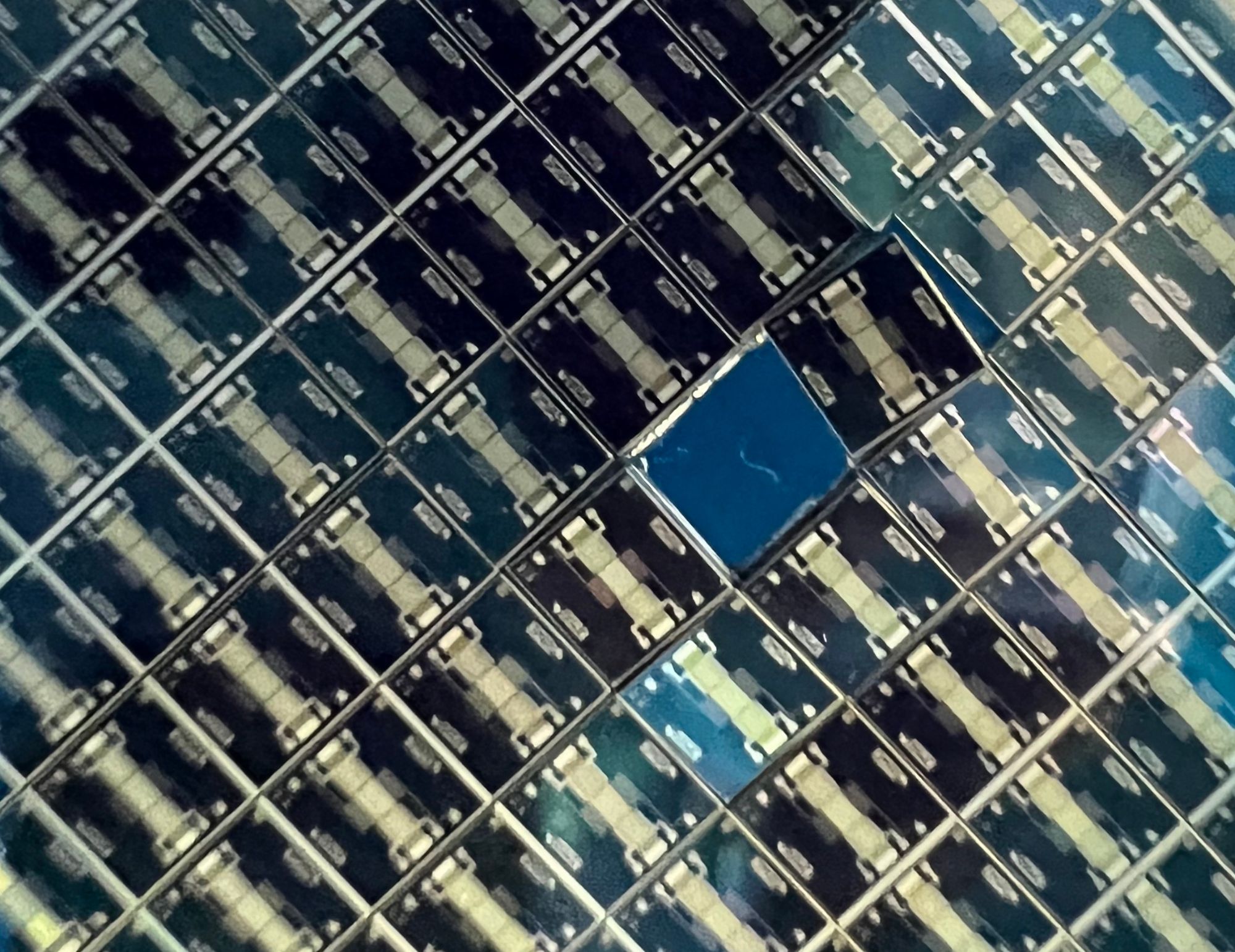
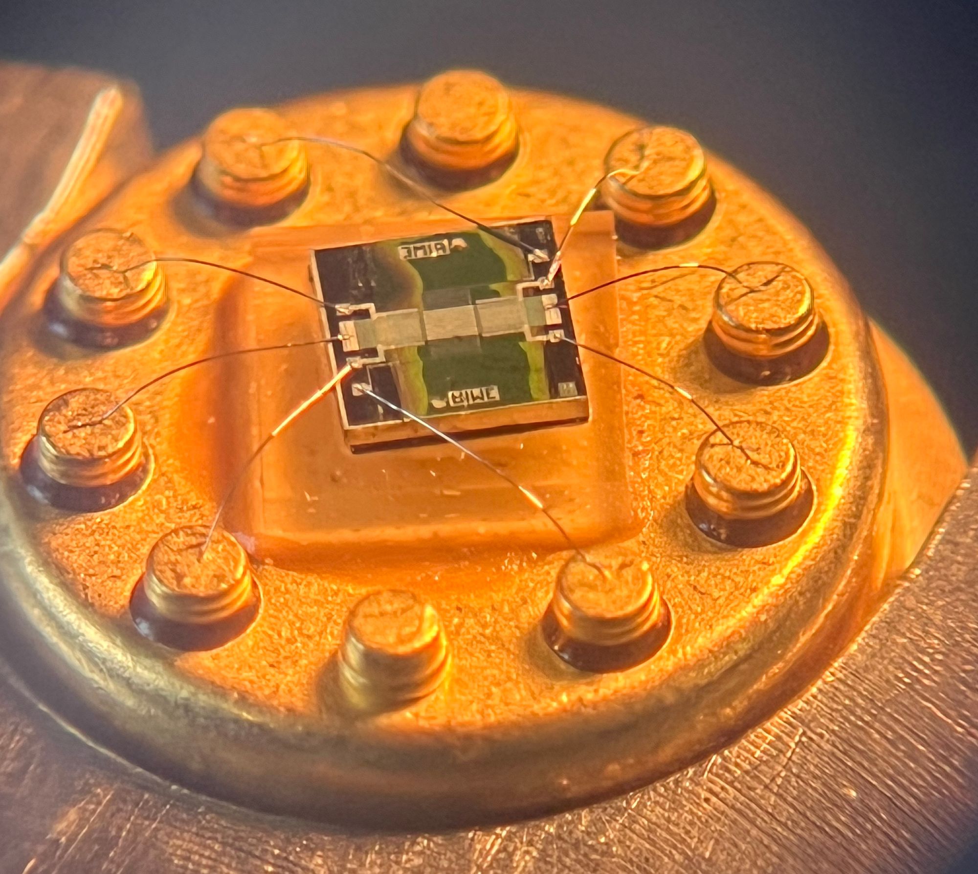
For more details, information on the practical work can be found here.
Nanoparticles synthesis & deposit
The first chemical reaction is the hydrolysis-condensation of Na2WO4, which is the conjugated base of tungstic acid. Once acidified, the unstable tungstic acid rapidly condenses (loss of a water molecule) and forms a yellow precipitate of nanoscale particles of tungsten oxide (of undefined form and composition).
The second objective is the growth of the WO3 nanorods. Since the oven will be at 180°C and we use water as solvent, we need to perform the next reaction into a special vessel that hold high pressure.
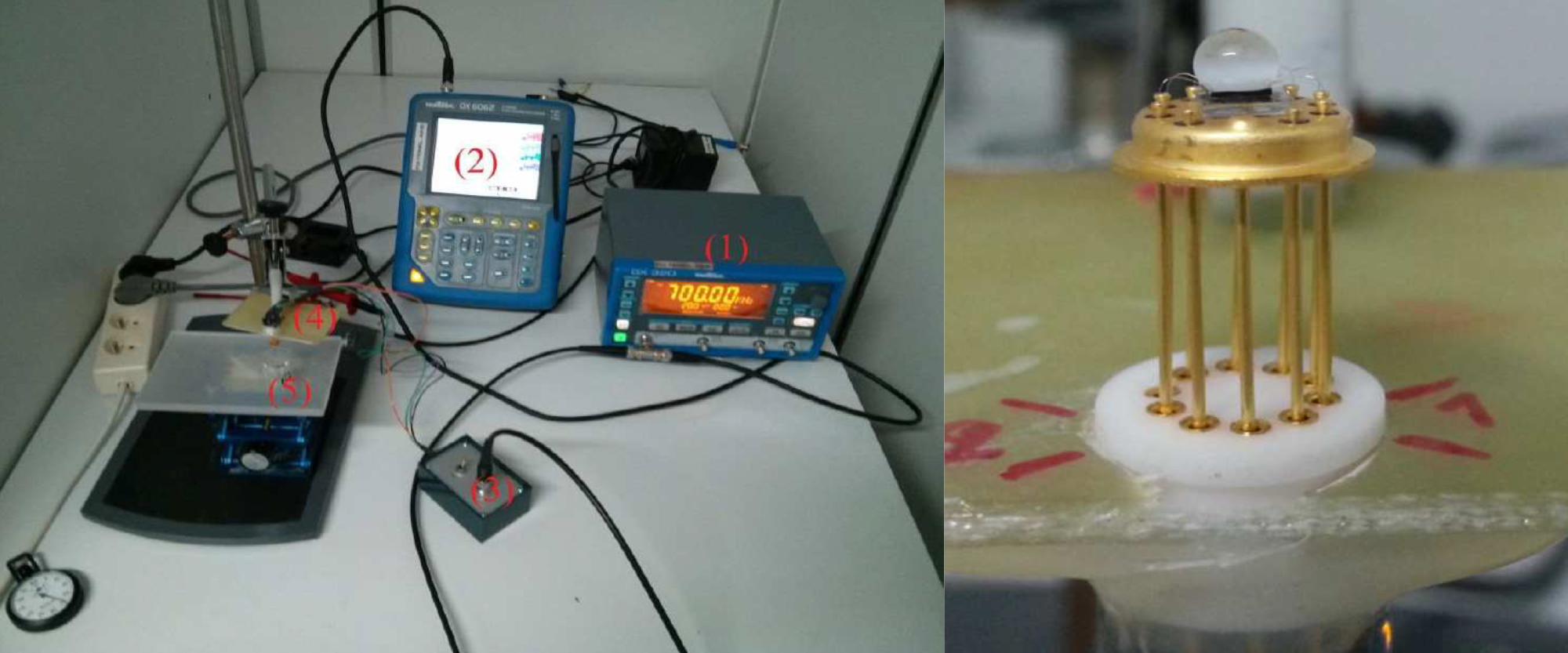
The last step is to apply a NPS selective deposition by dielectrophoresis. First, we connect one of the interdigitated electrodes to the AC generator. Then, carefully depose a drop of the nanoparticules solution (around 5 µl). Finally, we polarize the electrodes with a sinus voltage at 100 kHz (amplitude of 10 Vcc) and run the dielectrophoresis for 60s.
For more details, information on the practical work can be found here.